The NEORV32 is a Softcore Processor written entirely in VHDL and very well documented. In its default configuration, the only memory utilized for instruction and data memory is the on-chip FPGA RAM. This is a reasonable choice because the use of off-chip memory, such as DDR, requires proprietary intellectual property (IP) from the FPGA Vendor. The NEORV32's utilization of solely on-chip FPGA memory (BRAM), as inferred by its platform-independent VHDL code, enables its deployment across a diverse array of FPGA platforms.
The objective of this project is to establish a connection between the NEORV32 and the external DDR3 memory of the Arty A7-100T FPGA board. The NEORV32 softcore is capable of addressing 32 bits of memory space (4GB), which is sufficient to integrate the 256MB of DDR3 memory into its memory space.

The block diagram of the Vivado Project is illustrated in the accompanying image. The NEORV32 Softcore, more specifically the AXI_Lite Wrapper which can be found here, is instantiated as an IP module. Communication with the DDR PHY is controlled via the Memory Interface Generator IP (MIG). It is supplied with a reference clock (clk_ref_i) of 200 MHz and a system clk (sys_clk_i) of 166.67 MHz. The aforementioned clocks are generated by the Clocking Wizard IP module. The MIG generates a clock itself, ui_clk, which serves as the clock input for all other Modules used.
The NEORV32 Softcore is connected to an AXI Smartconnect module which facilitates the connection of multiple AXI Slaves to the AXI Master port of the processor. In this illustration, the Softcore is connected to the MIG, which in turn is linked to the DDR3 RAM, and to an AXI_GPIO IP Module.
In order to make these Modules accessible to the Softcore and the Software running on it, the DDR RAM and the GPIO Module have to be mapped into the address space of the Processor. NEORV32 has 32 address bits and can therefore address up to four GB of memory so it is more than capable to incorporate the 256 MB of external DDR RAM. The following image depicts the address space of the NEORV32 Processor:
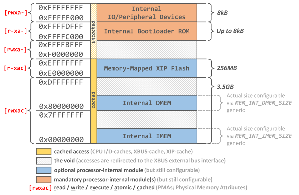
Some memory regions are reserved for processor internal memories like the bootloader or the internal data and instruction memory. But a lot of memory space is no preoccupied and therefore free to be used. As stated in the documentation a memory access to one of these "void" regions will be redirected to the external memory bus.
The address map of the modules used in this example project is listed in the following table:
| Memory Map | Start Address | Size | High Address |
|---|---|---|---|
| DDR | 0x1000_0000 | 256M | 0x1FFF_FFFF |
| GPIO | 0x4000_0000 | 64K | 0x4000_FFFF |
This memory map is configured via the AXI Smartconnect
So a write to address 0x10000000 is forwarded to the external memory bus which is then routed through the AXI Smartconnect to the MIG IP where it is sent to the DDR PHY. With the provided bus_explorer example, located in neorv32/sw/example/bus_explorer, the funcionality of the project can be tested by writing and reading memory locations located within the address map of the DDR.
The first three LED's of the Arty A7 are also memory mapped via the AXI_GPIO Module. So if you write the byte 0x01 to address 0x4000_0000 the first LED will light up and so on.
(The fourth LED is connected to the init_calib_done signal of the mig and indicates that the calibration of the ddr memory is finished)
This integration of the external DDR memory is more a proof of concept and can't be used conveniently with compiled C code because the processor will use it's enabled internal IMEM and DMEM. In a future project I plan to use the external DDR as the main memory of the Softcore and evaluate the performance differences.
Vivado v2020.2 is used in this project. To create the project files, execute following command:
vivado -mode batch -source neorv32_arty_ddr.tcl -nojournal -nolog


